Understanding the 8085 Architecture
The 8085 microprocessor is a 8 bit processor launched by Intel corporation in year 1976 . The 8085 microprocessor was developed using the NMOS technology . The NMOS stands for negative channel metal oxide semiconductor which is a type of technology used to manufacture IC chips. The 8085 processor is available in the market in many versions and.
TechExperts Intel 8085 Block Diagram
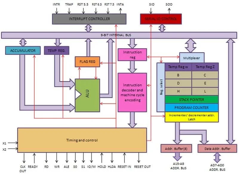
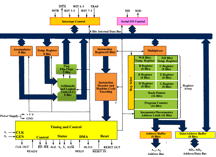
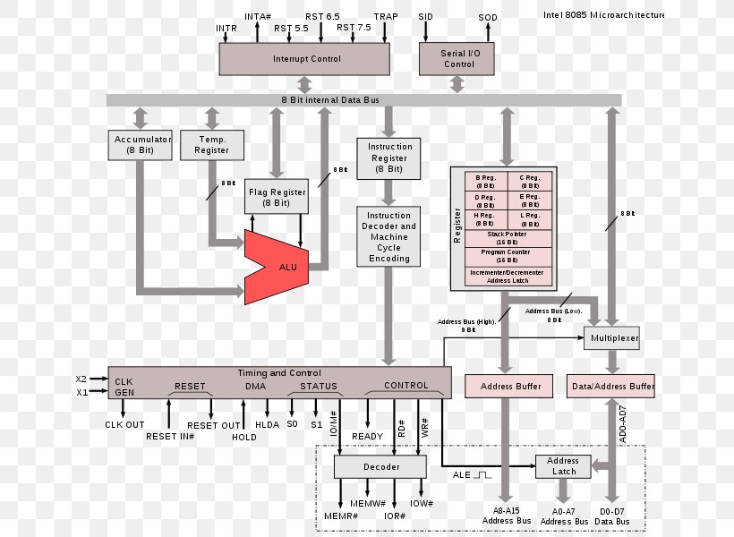
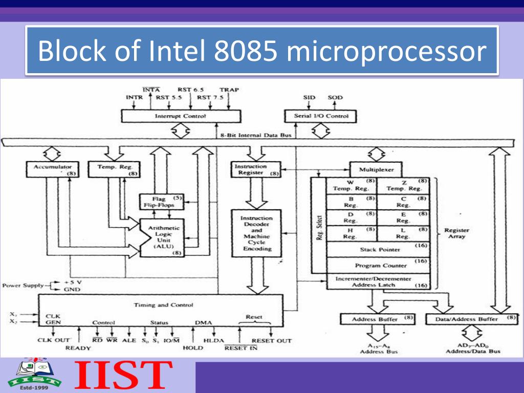
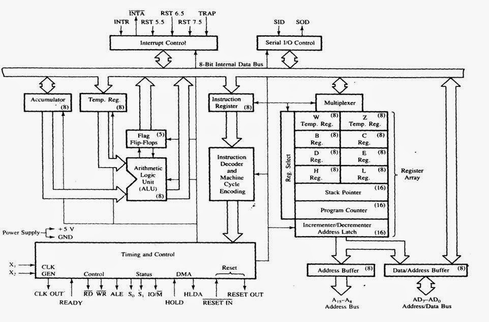
The block diagram of 8085 microprocessor provides a simplified and comprehensive view of its internal structure, showcasing how various components interact to perform complex tasks. This microprocessor is an 8-bit microprocessor and has components like an Arithmetic and Logic Unit (ALU), Registers, and Control Unit, Which work together to.
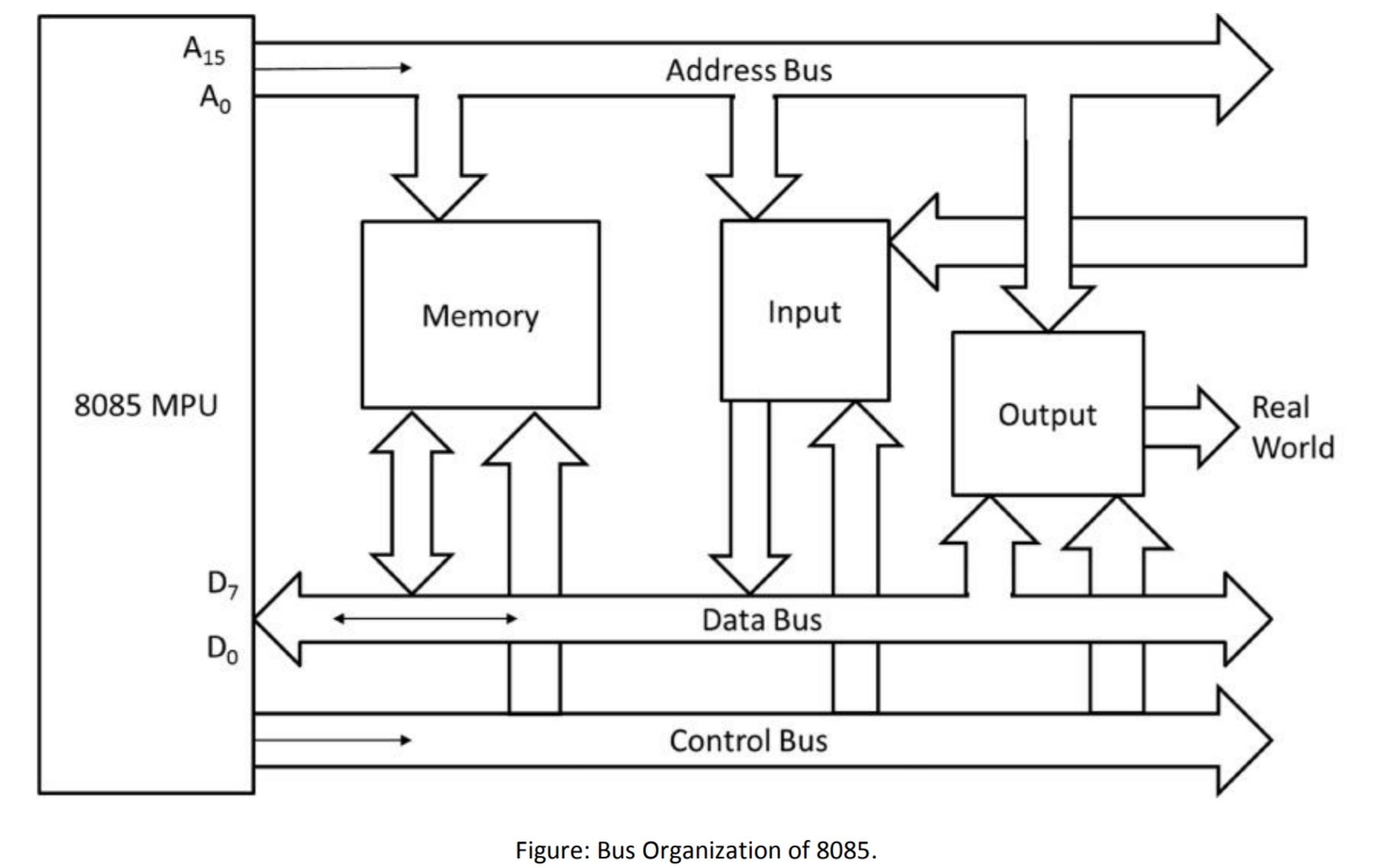
Bus Organization of 8085 Microprocessor ICT BYTE
by Sreejith Hrishikesan • June 30, 2019. 0. The internal architecture (Functional Block Diagram of 8085 Microprocessor) is shown in figure. The following are the functional blocks in the 8085 Microprocessor. 1. Accumulator. 2. Temporary register. 3.
Intel 8085 Microprocessor Block Diagram, PNG, 664x600px, Intel, Address Bus, Addressing Mode
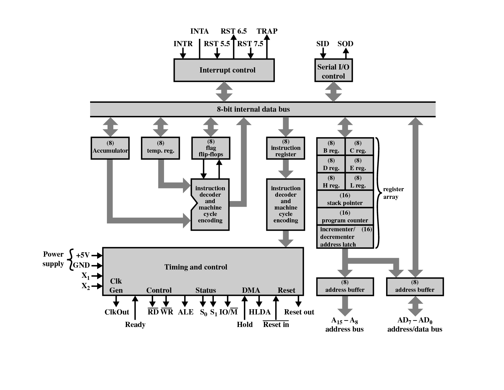
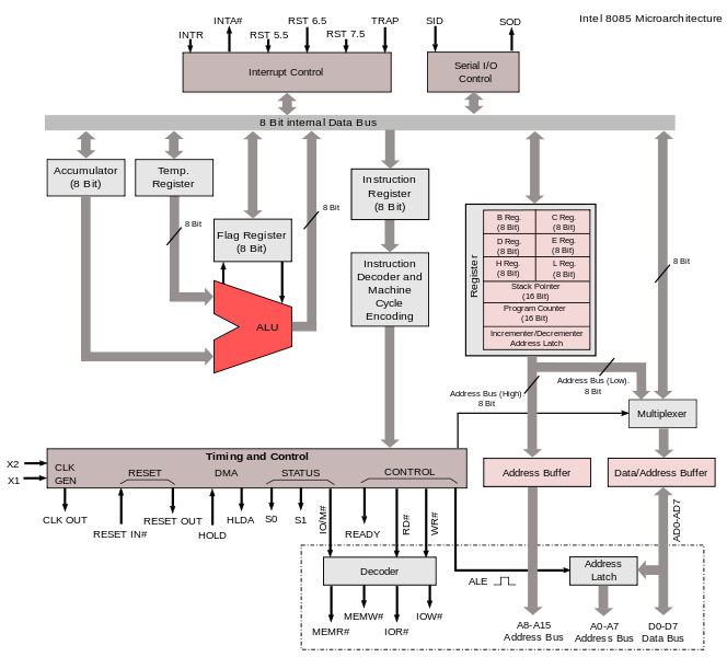
The Intel 8085 is an 8-bit microprocessor. Its data bus is 8-bit wide and therefore, 8 bits of data can be transmitted in parallel from or to the microprocessor. The Intel 8085 requires an address bus of 16-bit wide as the memory addresses are of 16-bits. The 8 most significant bits of the address are transmitted by the address bus, A-bus (pins.
PPT 8085 processor PowerPoint Presentation, free download ID4551641
The 8085 microprocessor is an 8-bit microprocessor. It consists of a 40-pin I.C. package and is fabricated on a single LSI chip. The Intel 8085 only uses a single +5v dc supply for its operation. The clock speed of the microprocessor is about 3MHz and the clock cycle is 320 ns. The time for the clock cycle of Intel 8085AH-2, the version is 200 ns.
Architechture of 8085
Functional block diagram of Intel 8085 microprocessor and the functional units. The 8085 is an 8-bit processor since its data length and data bus width are 8-bits. It has an addressing capability of 16 bits, that is, it can address 2 16 =64 KB of memory. The 8085 processor is generally available as a 40-pin IC package and uses+5V for power.

Microprocessor 8085 Block Diagram and Architecture ETechnoG
Block Diagram & Architecture Of 8085 Microprocessor Watch More Videos at: https://www.tutorialspoint.com/videotutorials/index.htmLecture By: Gowthami Swarna,.

Architecture of 8085 Microprocessor Bench Partner
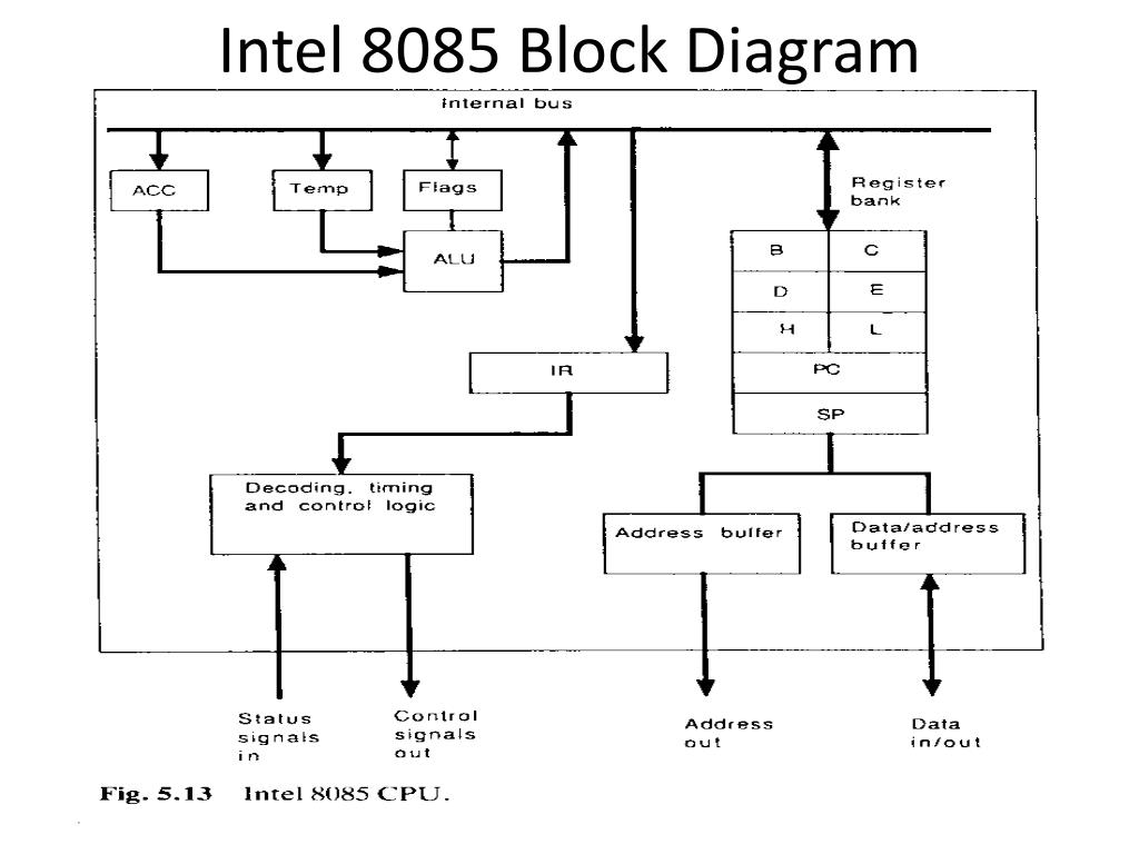
BLOCK DIAGRAM OF INTEL 8085 GURSHARAN SINGH TATLA [email protected] 1 Gursharan Singh Tatla [email protected] www.eazynotes.com Introduction to 8085 It was introduced in 1977. It is 8-bit microprocessor. Its actual name is 8085 A. It is single NMOS device. It contains 6200 transistors approx. Its dimensions are 164 mm x 222 mm.
PPT Understand the architecture of Intel 8085 microprocessor PowerPoint Presentation ID3541689
Pin Diagram. This 8085 is a 40-pin microprocessor where these are categorized into seven groups. With the below 8085 microprocessor pin diagram, the functionality and purpose can be known easily. 8085 Pin Diagram Data Bus. The pins from 12 to 17 are the data bus pins which are AD 0 - AD 7, this carries the minimal considerable 8-bit data and.
Microprocessors and Microcontrollers 8085 Microprocessor
The 8085 Microprocessor is one of the most popular microprocessors. In this article we look at some of the basic features and pin-out configuration of this microprocessor. The block diagram of the 8085 microprocessor is shown below: Figure 1.0 Block diagram of 8085 microprocessor
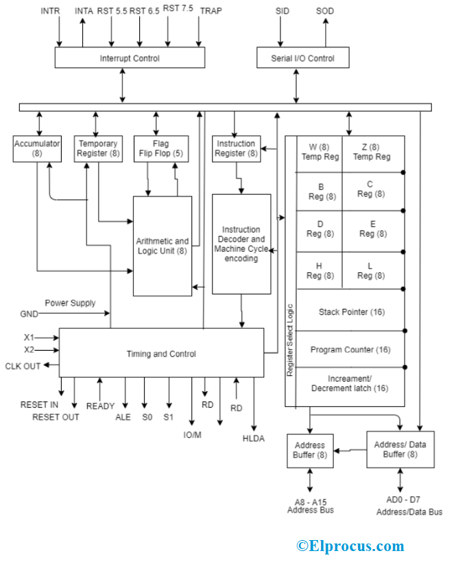
8085 Microprocessor Architecture Features and Its Working
It the main register of microprocessor. It is also called register 'A'. It is an 8-bit register. It is used in the arithmetic and logic operations. It always contains one of the operands on which arithmetic/logic has to be performed. After the arithmetic/logic operation, the contents of accumulator are replaced by the result.

Notes For You Intel's 8085 and its Architecture
8085 is an 8-bit microprocessor as it operates on 8 bits at a time and is designed with N-MOS technology. In this article you will get to know about the definition, architecture, block diagram and working of 8085 Microprocessor.

WORLD OF EMBEDDED Intel 8085 microprocessor & Architecture
The Architecture of the 8085. Before we begin with the main architectural block diagram of the 8085, let us discuss the key features of this processor. The Intel 8085 is an 8-bit general-purpose microprocessor. It has an 8-bit data bus. This means that 8 bits of data can flow around in the innards of the microprocessor.
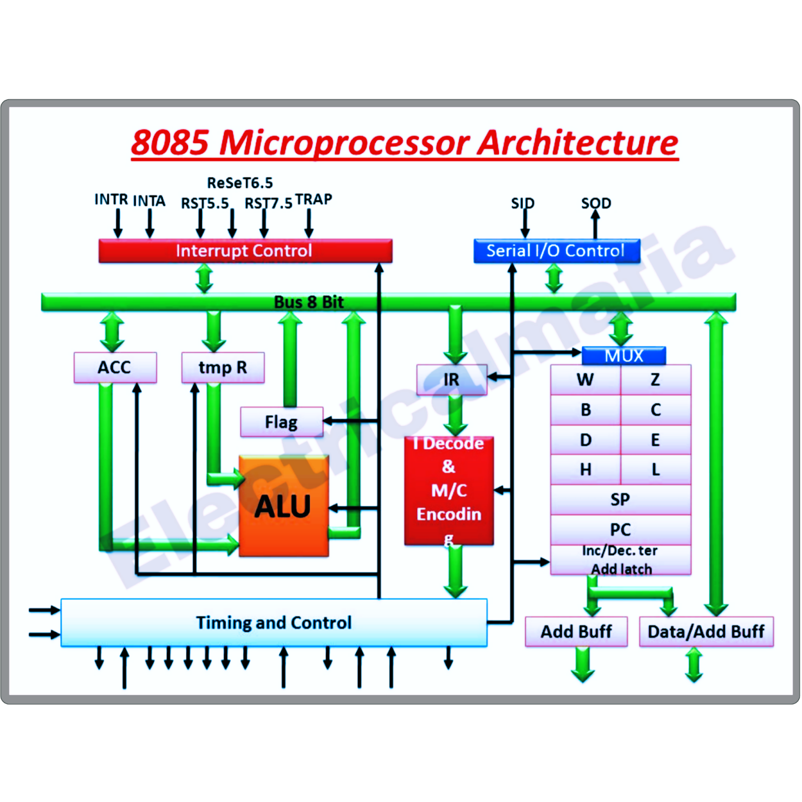
Architecture of 8085 microprocessor ElectricalMafia
Microprocessor - 8085 Architecture. 8085 is pronounced as "eighty-eighty-five" microprocessor. It is an 8-bit microprocessor designed by Intel in 1977 using NMOS technology. It has the following configuration −. 8-bit data bus. 16-bit address bus, which can address upto 64KB. A 16-bit program counter.

The Architecture of 8085 Microprocessor Microprocessors Tutorials Teachics
Timing Diagram and machine cycles of 8085 Microprocessor Timing Diagram Timing Diagram is a graphical representation. It represents the execution time taken by each instruction in a graphical format. The execution time is represented in T-states. Instruction Cycle: The time required to execute an instruction is called instruction cycle.
8085 Microprocessor Architecture, Features and Its Working
The 8085 microprocessor is an 8-bit microprocessor that was developed by Intel in the mid-1970s. It was widely used in the early days of personal computing and was a popular choice for hobbyists and enthusiasts due to its simplicity and ease of use. The architecture of the 8085 microprocessor consists of several key components, including the.